

Innovation
Single Crystal Doped POI Wafers
Single Crystal Piezo on insulator from 10nm to 1000nm thickness range
Tight Piezo stress control for superior K²eff distribution
Wafer transfer process
Scandium doped AlN up to 35% in mono-crystal form
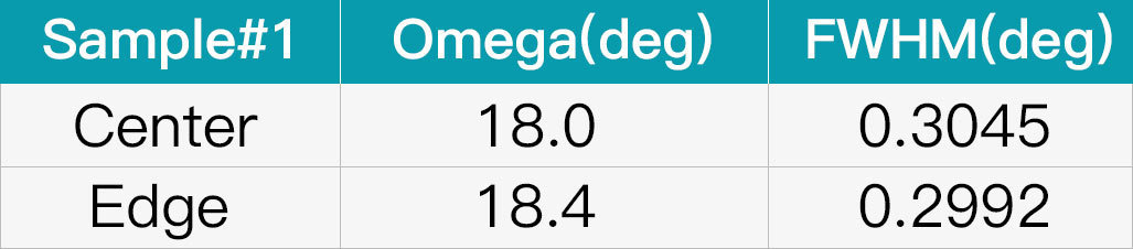
Sub 1nm (1S) Piezo thickness Uniformity on Wafer


Advanced Packaging
◼ Patented Ultra-Thin CSP — Matched FBAR devices with Sub 0.4mm thickness
◼ Patented WLP with Bump-on-Via (BoV) Structure — No TSV, No RDL
◼ Large ECO System for Advanced Packaging — FBAR Device in SAW Packaging
◼ Ultra-thin Coreless Laminates — Best-in-Class Layer Count to Thickness Ratio
Super IDM
◼ CRT has its own design, process front-end, process back-end and RF test teams.
◼ CRT Manufactures its own Single-Crystal Wafers in its TJ APC FAB
◼ CRT Tailors its Wafer Composition by collaboration of its Design, Process & Test Teams.
◼ CRT Process Team has Complete know-how for its FEOL/BEOL, MEMS and WLP Process.
Copyright © 2023 All Rights Changzhou Crystal Resonance Technologies Co., Ltd. Powered by www.300.cn


